|
Choosing AMB Ceramic Substrates for SiC Power Devices
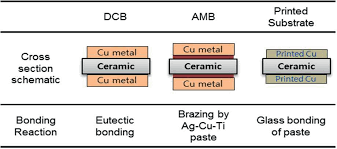
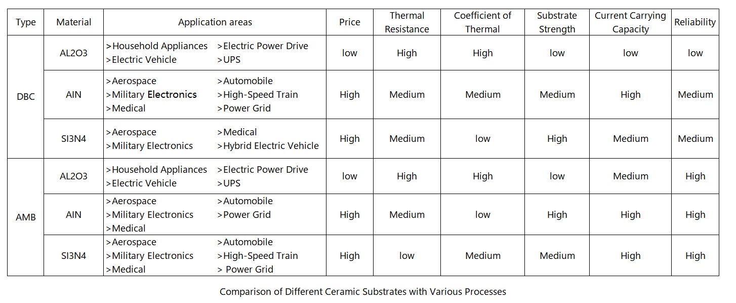
Ceramic substrates are categorized primarily into DBC (Direct Bond Copper), AMB (Active Metal Brazing), DPC, HTCC, LTCC, differentiated by their manufacturing processes and materials such as aluminum oxide (Al2O3), aluminum nitride (AlN), and silicon nitride (Si3N4). While aluminum oxide (Al2O3) is the most commonly used ceramic substrate with DBC technology, aluminum nitride (AlN) exhibits higher thermal conductivity, suitable for both DBC and AMB processes. Silicon nitride (Si3N4), known for its excellent reliability, is predominantly processed using the AMB technique.
Challenges with Traditional DBC Ceramic Substrates
Direct Bond Copper (DBC) ceramic substrates are produced using eutectic bonding, where copper and ceramics (Al2O3 or AlN) expand differently under high temperatures. This mismatch often leads to significant thermal stress, causing delamination of the copper layer from the ceramic surface. As a result, traditional DBC ceramic substrates struggle to meet the high-temperature, high-power, high-reliability packaging requirements.
The Role of Active Metal Brazing (AMB) Substrates
AMB substrates involve applying active brazing materials through thick-film printing or as solder sheets on the surface of ceramic carriers. Copper foils are then placed on both sides of the ceramic carrier coated with metal brazing materials, forming a structure of copper-brazing material-ceramic-brazing material-copper. Through stacking and vacuum sintering processes, ceramics, brazing materials, and copper foils are tightly bonded. Subsequent steps include exposure, development, etching, and surface treatments to produce the final product.
|